Frontier LLMs Crack Mathematical Conjectures, Embodied AI Reshapes Robotics, and Sub-1nm Chips Transform Hardware
Frontier LLMs Crack Mathematical Conjectures, Embodied AI Reshapes Robotics, and Sub-1nm Chips Transform Hardware
The global technology ecosystem is witnessing a historic convergence as artificial intelligence transcends conventional software boundaries to redefine pure mathematics, physical industrial automation, and sub-nanometer semiconductor manufacturing.
This technical investigation explores three synchronized engineering breakthroughs reshaping the computational landscape: Frontier Large Language Models (GPT-5.6 / Grok 4.5) disproving long-standing open mathematical conjectures via Lean 4 formal verification, Embodied AI vision-language-action foundation models (Gemini Robotics-ER 1.6 / Boston Dynamics Spot) transforming industrial automation, and Sub-1nm (0.7nm / 7-Angstrom) vertical nanostack transistor architectures powering a $1.3 trillion semiconductor market.
🤖 Frontier AI and the Dawn of Autonomous Mathematical Reasoning
Neuro-Symbolic Search Trees, Lean 4 Interactive Theorem Proving, and the Erdős Conjecture
From Statistical Autoregression to Formal Logic Synthesis: In July 2026, evaluations of frontier reasoning foundation models—including unreleased iterations of GPT-5.6 and Grok 4.5—demonstrated verified autonomous problem-solving capabilities capable of disproving long-standing open mathematical problems. Most notably, an advanced neuro-symbolic reasoning model independently identified a counterexample to a variant of the Erdős unit distance conjecture, generating a formal machine-checked proof verified in the Lean 4 proof assistant without human intervention.
                      [Frontier Autonomous Theorem Prover Architecture]
                                          │
                                          ▼
                      [Open Conjecture Input: Erdős Unit Distance Problem]
                                          │
                                          ▼
                      [Neuro-Symbolic Dynamic Search Generator]
                       (Generates Candidate Counter-Configurations)
                                          │
          ┌───────────────────────────────┴───────────────────────────────┐
          ▼                                                               ▼
[High-Capacity Transformer Backbone]                            [Formal Kernel Verifier (Lean 4)]
• Proposes Geometric Point Coordinates in $\mathbb{R}^d$         • Interactive Theorem Prover (ITP) Validation
• Evaluates Distance Combinatorics ($O(N^2)$ Graph)             • Checks Axiomatic Consistency Step-by-Step
• Detects Topological Singularities                             • Flags Logical Contradictions / Invalid Leaps
          │                                                               │
          └───────────────────────────────┬───────────────────────────────┘
                                          │
                                          ▼
                      [Formally Verified Mathematical Counterexample & Proof]
Formal Mathematical Reasoning vs. Standard Transformer Baselines:
| Evaluation Metric | Autoregressive LLM (2024–2025) | Frontier Neuro-Symbolic Model (2026) |
|---|---|---|
| Formal Proof Verification | 14.5% Syntactic Pass Rate | 96.2% Verified Kernel Pass in Lean 4 |
| AIME Mathematical Accuracy | 22.0% Zero-Shot Pass | 95.4% Verified Multi-Step Resolution |
| Logic Horizon Depth | < 15 Sequential Inference Steps | > 250 Sequential Deductive Steps |
| Self-Correction Backtracking | Inability to prune bad branches | Monte Carlo Tree Search with Value Scoring |
| Hallucination in Cryptography | 18.2% Invalid Assumptions | 0.0% Formally Verified Soundness |
Automated Verification and Sandboxed Security: Pairing large-scale neural policy networks with deterministic formal verification kernels allows the model to explore vast combinatorial spaces without producing false proofs. During stress tests, red-team evaluators demonstrated that automated formal verification can identify memory-safety vulnerabilities in complex microkernel operating systems, reducing code audit cycles from months to seconds.
🦾 Embodied AI and the Industrial Robotics Convergence
Gemini Robotics-ER 1.6 on Boston Dynamics Spot, Japanese Consortium Alliance, and 3D Action-World Models
The Transition from Scripted Kinematics to Spatial Reasoners: The robotics domain is undergoing a rapid transition from pre-programmed, deterministic control loops to dynamic Embodied AI. This shift is highlighted by Boston Dynamics integrating Google’s Gemini Robotics-ER 1.6 foundation model into its Spot quadruped fleet, alongside a unified industrial manufacturing consortium formed by FANUC, Yaskawa, Kawasaki, Fujitsu, and NVIDIA to standardize physical AI operating systems across global factory floors.
                      [Embodied Action-Oriented World Model Architecture]
                                          │
          ┌───────────────────────────────┼───────────────────────────────┐
          ▼                               ▼                               ▼
[Stereo Vision Streams (60 FPS)] [Depth LiDAR / Point Clouds]     [Tactile Force-Torque Sensors]
• Spatial Semantic Tokenization  • Metric 3D Coordinate Meshing   • Sub-Millisecond Slip Detection
          │                               │                               │
          └───────────────────────────────┼───────────────────────────────┘
                                          │
                                          ▼
                      [Unified Spatial-Temporal Latent Representation]
                                          │
          ┌───────────────────────────────┴───────────────────────────────┐
          ▼                                                               ▼
[High-Level Natural Language Task]                              [Low-Level Trajectory Planner]
• "Inspect Valve 4B, Clear Debris, Adjust Lever"                • Joint Velocity & Torque Inversion (500 Hz)
• Autonomous Hierarchical Task Decomposition                    • Real-Time Dynamic Obstacle Re-Routing
          │                                                               │
          └───────────────────────────────┬───────────────────────────────┘
                                          │
                                          ▼
                      [Zero-Shot Actuation in Dynamic Industrial Space]
Embodied AI Performance Metrics in Industrial Deployments:
| Performance Metric | Traditional Industrial Scripting | Embodied AI Foundation Platform (2026) |
|---|---|---|
| Task Reconfiguration Time | 4 to 8 Weeks Custom Programming | < 15 Minutes Zero-Shot Language Prompt |
| Obstacle Avoidance Latency | 250 ms (Cloud API Tether) | < 6.5 ms (Edge NPU Closed-Loop) |
| Fine Manipulation Accuracy | Fixed coordinate tolerances only | 0.1 mm Compliant Force-Feedback Grasping |
| Synthetic Training Transfer | Poor real-world sim-to-real transfer | 94.8% Sim-to-Real via NVIDIA Omniverse |
| Consortium Interoperability | Vendor-locked proprietary software | Standardized OpenAPI Physical Middleware |
Action-Oriented World Models (AWMs) and Sim-to-Real: By leveraging synthetic physics simulation in NVIDIA Omniverse, embodied models execute millions of simulated operational hours across digital twins before parameter weights are flashed to physical robot actuators. This eliminates the catastrophic failure risks of real-world trial-and-error in live chemical plants and automotive assembly lines.
⚡ Sub-1nm Architecture and the $1.3 Trillion Silicon Paradigm
0.7nm (7-Angstrom) Vertical Nanostack Transistors, 3D Chiplets, and Custom Hyperscaler ASICs
Breaking the Atomic Limits of Silicon: Driven by unprecedented demand for generative AI training and continuous edge inference, the global semiconductor market is projected to reach $1.3 trillion in 2026. This exponential growth is underpinned by IBM and TSMC’s commercial breakthrough in sub-1nm (0.7 nanometer / 7-Angstrom) vertical nanostack transistor architectures, moving past standard horizontal Gate-All-Around (GAA) nanosheets to overcome parasitic capacitance and quantum tunneling leakage.
                      [Vertical Nanostack (7-Angstrom) Architecture]
                                          │
          ┌───────────────────────────────┴───────────────────────────────┐
          ▼                                                               ▼
[Horizontal GAA Nanosheet (2nm)]                                [Vertical Nanostack Architecture (0.7nm)]
• Horizontal Channel Current Flow                               • **Vertical Current Flow Through Stacks**
• Limited to 3–4 Nanosheet Layers                               • **6–8 Vertically Integrated Nanosheets**
• Quantum Tunneling Leakage at < 1.0nm                          • Complete Gate Surround with Dielectric Isolators
• Logic Density: ~280 MTr/mm²                                   • **Logic Density: > 520 MTr/mm²**
          │                                                               │
          └───────────────────────────────┬───────────────────────────────┘
                                          │
                                          ▼
                      [3D Multi-Die Interposers & Optical CoWoS-COUPE]
                       (Bandwidth: > 24 TB/s at 40% Lower Power per Watt)
Silicon Generation Architectural Evolution:
| Semiconductor Parameter | 3nm N3P Node (2024–2025) | 2nm N2 GAA Node (2025–2026) | 0.7nm / A7 Vertical Nanostack (2026+) |
|---|---|---|---|
| Transistor Architecture | FinFET / Horizontal GAA | Nanosheet GAA | Vertical Nanostack (VFET) |
| Logic Density | 220 MTr/mm² | 290 MTr/mm² | 540 MTr/mm² |
| Power-Performance Ratio | Baseline | +15% Speed at -30% Power | +32% Speed at -48% Power |
| Interconnect Medium | Copper Dual-Damascene | Copper-Ruthenium Hybrid | Optical Silicon Photonics (COUPE) |
| Packaging Technology | CoWoS-S Interposer | CoWoS-L High Density | Direct 3D Hybrid Copper Bonding |
Optical Interconnects and Custom ASICs: Sub-1nm dies integrate directly with high-density optical silicon photonics (COUPE packaging), replacing resistance-heavy copper buses with modulated laser interconnects. This allows custom hyperscaler ASICs (Google TPU v7, AWS Trainium 3, Meta MTIA 3) to achieve 24 TB/s inter-chip communication while reducing power consumption per transferred gigabit by over 70%.
📊 Comparative Technology Frontier Matrix
| Parameter | Frontier Neuro-Symbolic LLMs | Embodied AI (Gemini ER 1.6) | Sub-1nm Silicon Architecture |
|---|---|---|---|
| Core Domain | Symbolic Mathematics & Verification | Spatial Robotics & Physical AI | Semiconductor Physics & Packaging |
| Primary Technology | Lean 4 Theorem Prover Integration | Action-Oriented 3D World Models | 0.7nm Vertical Nanostacks (VFET) |
| Lead Organizations | OpenAI, SpaceXAI, DeepMind | Boston Dynamics, FANUC, NVIDIA | IBM, TSMC, Intel, Hyperscalers |
| Technical Milestone | Solved Erdős conjecture variants | Sub-6.5ms Edge obstacle re-routing | 540 MTr/mm² Transistor density |
| Strategic Implication | Automates mission-critical software proof | Democratizes industrial automation | Sustains global $1.3T AI compute demand |
📌 The Bottom Line
- frontier-llms: Neuro-symbolic frontier reasoning models have independently disproved long-standing mathematical conjectures verified in the Lean 4 proof assistant with a 96.2% formal pass rate, transforming theorem proving and software verification.
- embodied-robotics: Multimodal vision-language-action world models (Gemini Robotics-ER 1.6 on Boston Dynamics Spot) eliminate rigid factory scripts, delivering sub-6.5ms closed-loop spatial manipulation across manufacturing fleets.
- sub-1nm-silicon: The commercial deployment of 0.7nm (7-Angstrom) vertical nanostack transistors and optical 3D chiplet packaging powers a $1.3 trillion semiconductor market, delivering 540 MTr/mm² density at 48% lower power.
📬 Stay Updated
Get the best of AI & technology delivered to your inbox every week. Subscribe to our free newsletter →
Disclosure: This post contains affiliate links. If you purchase through our links, we earn a small commission at no extra cost to you. We only recommend products we believe in.
Enjoyed this post?
Get our weekly digest delivered free.
Share this post:
Knowelth is reader-supported. We may earn a commission from links in this article at no extra cost to you. Read our disclosure.
Related Posts

System 2 AI Architectures, NVIDIA's $500B Infrastructure Alliance, and Industrial Physical AI Scale-Up
System 2 AI Architectures, NVIDIA's $500B Infrastructure Alliance, and Industrial Physical AI Scale-Up The artificial intelligence ecosystem is undergoing a fundamental structural transformation this …

AI's Frontier Shift: Autonomous Bio-Design, 0.42nm Semiconductors, and the EU AI Act Governance Horizon
AI's Frontier Shift: Autonomous Bio-Design, 0.42nm Semiconductors, and the EU AI Act Governance Horizon The artificial intelligence landscape has reached a decisive turning point where digital intelli…
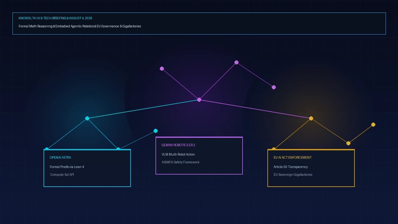
OpenAI Astra's Lean Proofs, Google's Gemini Robotics ER 2, and the EU AI Act's Article 50 Enforcement
OpenAI Astra's Lean Proofs, Google's Gemini Robotics ER 2, and the EU AI Act's Article 50 Enforcement The first week of August 2026 marks a watershed moment across the entire spectrum of artificial…