Tata Electronics & Dholera Fab: India's Chip Ambition
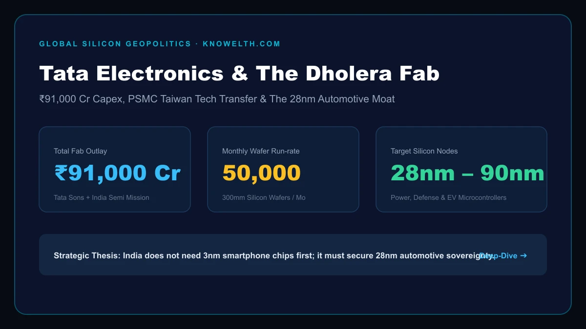
Tata Electronics & The Dholera Fab: Can India Break Taiwan's Semiconductor Monopoly?
Quick Summary: In the arid plains of Dholera Special Investment Region (SIR) in Gujarat, Tata Electronics, in technological partnership with Taiwan's Powerchip Semiconductor Manufacturing Corporation (PSMC), is erecting India's first commercial mega-semiconductor fabrication facility. Backed by a staggering ₹91,000 Crore ($11 Billion) capital expenditure and subsidized up to 70% under the central India Semiconductor Mission (ISM) and state incentives, the Dholera fab targets an initial run-rate of 50,000 300mm wafer starts per month. While Western media frequently fixates on cutting-edge 2nm and 3nm smartphone silicon monopolized by TSMC in Hsinchu, Tata's strategic decision to anchor in 28nm, 40nm, 55nm, and 90nm legacy and mature nodes represents a masterclass in sovereign industrial risk-mitigation: capturing the indispensable, high-margin automotive, power grid, telecommunications, and defense electronics that keep the physical economy running.
The Strategic Mature-Node Moat: Over 68% of the global automotive and industrial semiconductor bill-of-materials relies on mature nodes (28nm to 90nm). During the 2021–2022 chip crisis, global automakers lost over $210 billion in revenue not from missing 3nm AI processors, but from a shortage of $2 microcontroller chips manufactured on 55nm lines. By monopolizing domestic automotive and industrial wafer output, Tata creates an captive supply chain for Tata Motors, Jaguar Land Rover, and Indian defense manufacturers that foreign sanctions or Taiwan Strait blockades cannot disrupt.
+---------------------------------------------------------------------------------------------------+
|                        TATA DHOLERA FAB: STRUCTURAL ECOSYSTEM ARCHITECTURE                        |
+---------------------------------------------------------------------------------------------------+
                                                  │
         ┌────────────────────────────────────────┼────────────────────────────────────────┐
         ▼                                        ▼                                        ▼
+──────────────────────────+             +──────────────────────────+             +──────────────────────────+
| CAPITAL STACK (ISM)      |             | TECHNOLOGY TRANSFER      |             | CAPTIVE DEMAND OFF-TAKE  |
| • 50% Central Subsidy    |             | • PSMC (Taiwan) Partner  |             | • Tata Motors / JLR EVs  |
| • 20% Gujarat State Aid  |             | • 300mm (12-inch) Wafers |             | • Tejas Networks Telecom |
| • Tata Equity Cushion    |             | • 28nm Logic & 90nm PMIC |             | • Indian Defense & Space |
| • Net Capex Risk: Low    |             | • Full Cleanroom Cl. 1   |             | • Global Auto Tier-1s    |
+──────────────────────────+             +──────────────────────────+             +──────────────────────────+
         │                                        │                                        │
         └────────────────────────────────────────┼────────────────────────────────────────┘
                                                  ▼
+---------------------------------------------------------------------------------------------------+
| SYNTHESIS: Domestic Semiconductor Self-Sufficiency Shielding India's $300B Electronics Export Goal |
+---------------------------------------------------------------------------------------------------+
🏛️ 1. The Geopolitical Crucible: Why Dholera Matters Now
For three decades, the global semiconductor supply chain has operated under extreme geopolitical concentration. Taiwan Semiconductor Manufacturing Company (TSMC) manufactures over 90% of the world's most advanced processors and nearly 55% of all foundry output worldwide.
Under the India Semiconductor Mission (ISM), inaugurated with an initial sovereign commitment of ₹76,000 Crore, the Indian government identified silicon fabrication not merely as an industrial diversification play, but as a non-negotiable pillar of national defense and macroeconomic resilience.
Dholera was selected as the ground zero for this initiative due to three foundational infrastructure prerequisites:
- Uninterrupted Power Quality: Semiconductor lithography requires millisecond-level power stability. Voltage flickers lasting even 10 milliseconds can ruin an entire production lot of silicon wafers worth millions of dollars. Dholera is plugged into dedicated dual-circuit transmission grids tied directly to Gujarat's massive solar and renewable generation parks.
- Ultra-Pure Water (UPW) Supply: Manufacturing a single 300mm silicon wafer consumes between 8,000 to 10,000 liters of ultra-pure water (water stripped of all minerals, bacteria, and particulates down to the sub-part-per-billion level). Dholera leverages dedicated Narmada canal linkages paired with closed-loop multi-stage reverse osmosis and industrial water recycling facilities designed to recover over 85% of process effluent.
- Logistics & Seismic Stability: Dholera sits in Seismic Zone III, providing critical ground vibration damping essential for sub-micron photolithography steppers, while offering seamless access to Western dedicated freight corridors and Mundra/Kandla deep-water container ports.
+---------------------------------------------------------------------------------------------------+
|                            THE 300MM WAFER MANUFACTURING CYCLE AT DHOLERA                         |
+---------------------------------------------------------------------------------------------------+
 Raw Polysilicon Ingot ──► Slicing into 300mm Raw Wafers ──► Surface Oxidation & Chemical Cleaning
                                                                              │
                                                              ┌───────────────┘
                                                              ▼
 Ultra-Pure Water (UPW) Rinse ◄── Ion Implantation ◄── Photolithography (Immersion DUV Steppers)
              │
              └───────────────► Thin-Film Chemical Vapor Deposition (CVD) ──► Chemical Mechanical Polishing
                                                                              │
                                                              ┌───────────────┘
                                                              ▼
 Tested Finished Wafers ──► Shipped to Tata Electronics OSAT Facility (Jagiroad, Assam) for Packaging
+---------------------------------------------------------------------------------------------------+
📊 2. Comparative Matrix: Dholera vs Global Foundry Benchmarks
To understand where Tata Electronics fits into the global semiconductor hierarchy, it is vital to contrast its technical and operational metrics against the established giants of East Asia and North America:
+---------------------------------------------------------------------------------------------------+
|                     GLOBAL FOUNDRY CAPACITY & INFRASTRUCTURE BENCHMARK MATRIX                     |
+---------------------------------------------------------------------------------------------------+
| Parameter / Capability        | Tata Electronics (Dholera)       | TSMC (Taiwan / Fab 18)         | GlobalFoundries (Fab 8, NY)   |
+-------------------------------+----------------------------------+--------------------------------+-------------------------------+
| Target Silicon Process Nodes  | 🏆 28nm, 40nm, 55nm, 90nm        | 3nm, 5nm (Leading Edge)        | 12nm, 22nm, 28nm FD-SOI       |
| Initial Monthly Wafer Starts  | 50,000 (300mm Wafers)            | 130,000+ (300mm Wafers)        | 60,000 (300mm Wafers)         |
| Primary Technology Partner    | PSMC (Taiwan) Transfer Agreement | Proprietary Internal R&D       | Ex-AMD Manufacturing IP       |
| Government Capex Subsidy %    | 🏆 Up to 70% (Center + State)    | ~15%–25% (Taiwan Subsidies)    | ~30% (US CHIPS Act)           |
| Primary End Markets           | Automotive, EV, Telecom, Power   | Smartphones, HPC, Nvidia GPUs  | Aerospace, Defense, IoT, Auto |
| Packaging / OSAT Integration  | Captive Fab-to-OSAT (Assam Unit) | InFO / CoWoS Advanced Stacking | Third-Party OSATs (ASE, Amkor)|
| Commercial Production Target  | 2026–2027 Ramp-Up Phase          | Mature Commercial Operations   | Fully Scaled Production       |
+-------------------------------+----------------------------------+--------------------------------+-------------------------------+
⚙️ 3. The 28nm Strategic Geometry: Why Mature Nodes are Goldmines
Enjoyed this post?
Get our weekly digest delivered free.
The financial media frequently commits the error of equating semiconductor importance with transistor nanometer miniaturization. While leading-edge nodes (3nm, 2nm) capture headlines for powering iPhones and generative AI accelerators, they present extreme capital risk:
- Extreme Tooling Cost: A single ASML High-NA Extreme Ultraviolet (EUV) scanner costs in excess of $350 million. In contrast, 28nm and 40nm manufacturing utilizes mature Deep Ultraviolet (DUV) immersion lithography systems, where equipment costs are a fraction, secondary market machinery is accessible, and tool uptime routinely exceeds 98%.
- Infinite Product Lifecycles: An AI accelerator node is obsolete in 24 months. A 28nm automotive microcontroller, once qualified by Mercedes-Benz, Tata Motors, or Bosch, remains in active, recurring commercial production for 15 to 20 years without redesign.
- Impregnable Gross Margins: Once a 28nm/55nm cleanroom amortizes its initial capital equipment over a 5-year depreciation schedule, the marginal cost to fabricate an additional wafer falls drastically, while automotive customers continue paying premium prices for verified zero-defect reliability.
+---------------------------------------------------------------------------------------------------+
|                         THE MATURE SILICON VALUE STACK FOR TATA GROUP                             |
+---------------------------------------------------------------------------------------------------+
  Tata Motors / EV Powertrain ──► Battery Management Systems (BMS) Microcontrollers (28nm/40nm)
  Tata Power Renewable Grids  ──► High-Voltage Gallium Nitride / Silicon Carbide Power Switches
  Tejas Networks (Telecom)    ──► 5G Radio Access Network (RAN) Baseband Processing Chips
  Air India Fleet Avionics    ──► Flight Control Display & Cabin Power Management Silicon
+---------------------------------------------------------------------------------------------------+
📦 4. The Twin Engine: Jagiroad OSAT Facility in Assam
A silicon wafer emerging from a cleanroom in Dholera is not a usable chip; it must be diced, wire-bonded, capped in thermal resin, and tested under extreme thermal stress. This process—Outsourced Semiconductor Assembly and Test (OSAT)—is where Tata has established its second structural pillar.
Simultaneously with Dholera, Tata Electronics is executing a ₹27,000 Crore OSAT facility in Jagiroad, Assam. With an engineered daily packaging capacity exceeding 48 million semiconductor chips, the Assam facility will handle:
- Flip-Chip & Ball Grid Array (BGA) Packaging: Delivering high-density input/output interfaces for automotive telematics.
- Silicon Level Testing: Automated high-speed robotic parametric sorting guaranteeing zero automotive assembly-line failures.
- Captive Closed-Loop Integration: Wafers produced at Dholera fly via air corridors directly to Assam, keeping India's entire semiconductor intellectual and physical custody domestic.
🚧 5. Key Execution Risks & Headwinds
Despite monumental state backing, Tata Electronics faces four acute challenges that will dictate whether Dholera succeeds or becomes a capital trap:
- Yield Curve Learning Delay: In foundry economics, the percentage of non-defective dies per wafer (Yield) is the difference between operating profit and catastrophic cash burn. Mature fabs run at 92%+ yields. Achieving this requires months of precision tuning of chemical slurries, cleanroom airflow, and photolithographic masks.
- Deep Specialized Talent Shortage: India graduates hundreds of thousands of software developers, but possesses an acute shortage of physical cleanroom engineers, lithography process specialists, and wafer defect metrology experts. Tata is actively mitigating this through large-scale training rotations at PSMC fabs in Taiwan.
- Global Foundry Capacity Glut in 28nm: China (via SMIC and Hua Hong) has invested tens of billions of dollars into legacy 28nm and 40nm capacity. If China floods global markets with heavily subsidized mature chips, Tata must rely on domestic tariff moats and geopolitical "China+1" supply chain mandates from Western original equipment manufacturers.
📌 Strategic Case Study Takeaways for Business Leaders & Investors
+---------------------------------------------------------------------------------------------------+
|                                  STRATEGIC INDUSTRIAL LESSONS                                     |
+---------------------------------------------------------------------------------------------------+
| Strategic Vector               | Core Business & Capital Allocation Lesson                        |
+--------------------------------+------------------------------------------------------------------+
| Sovereign Subsidy Arbitrage    | Co-investing with state industrial policy eliminates 70% capex. |
| Mature-Node Market Selection   | Avoid prestige tech traps; target the boring, high-demand nodes. |
| Captive Demand Backstop        | Having internal conglomerate off-takers guarantees baseline run-rate. |
| Geopolitical Friend-Shoring    | Western auto OEMs will pay a premium for non-Taiwanese silicon.   |
+---------------------------------------------------------------------------------------------------+
📫 Corporate Intelligence & Technology Moats
Subscribe to Knowelth to receive weekly deconstructions of India's capital expenditure boom, industrial supply chain shifts, and semiconductor geopolitics.
Subscribe to Knowelth Executive Intelligence →
Disclaimer: This research report is compiled for institutional and corporate educational analysis and does not constitute financial advice or an endorsement to trade specific securities.
Technical architecture teardowns, artificial intelligence evaluations, and software benchmarks published on Knowelth reflect independent developer testing and publicly available documentation. We maintain complete editorial independence from vendor sponsorships. Read our Editorial Policy.
Enjoyed this post?
Get our weekly digest delivered free.
Share this post:
Knowelth is reader-supported. We may earn a commission from links in this article at no extra cost to you. Read our disclosure.
Related Posts
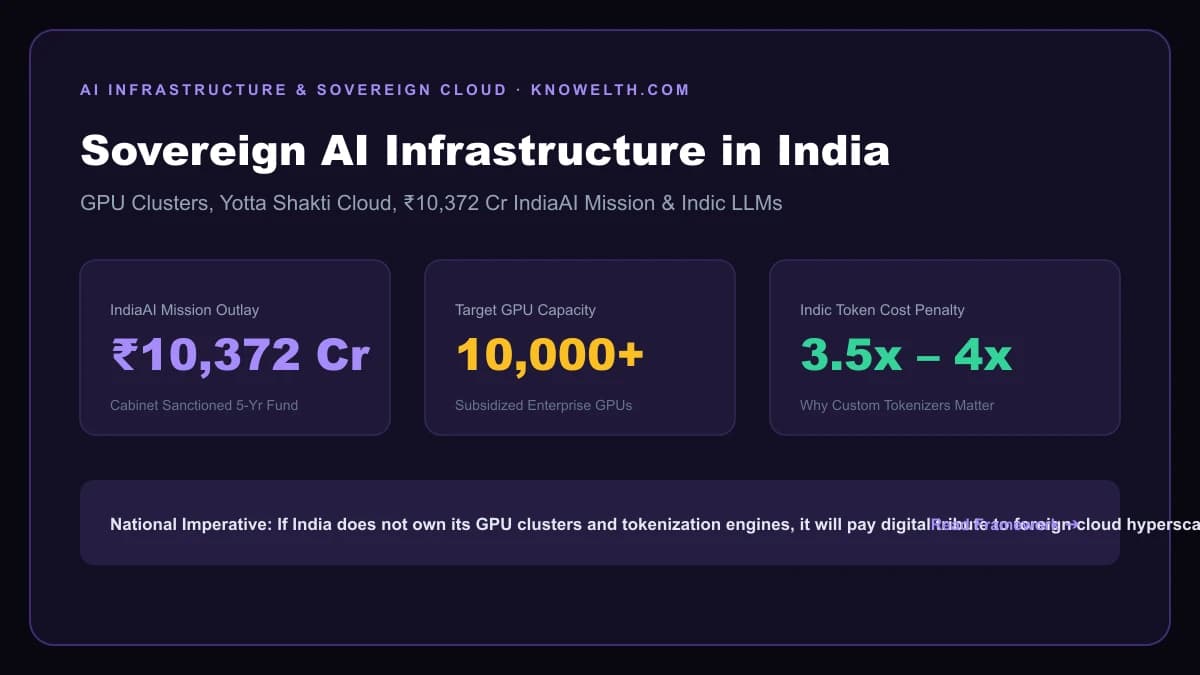
Sovereign AI India: GPU Cloud & Indic LLMs
Sovereign AI Infrastructure in India: GPU Clusters, Yotta Shakti Cloud, and Indic LLMs Quick Summary: In the global race for artificial intelligence hegemony, computing power has superseded crude oil …

System 2 AI Architectures, NVIDIA's $500B Infrastructure Alliance, and Industrial Physical AI Scale-Up
System 2 AI Architectures, NVIDIA's $500B Infrastructure Alliance, and Industrial Physical AI Scale-Up The artificial intelligence ecosystem is undergoing a fundamental structural transformation th…

AI's Frontier Shift: Autonomous Bio-Design, 0.42nm Semiconductors, and the EU AI Act Governance Horizon
AI's Frontier Shift: Autonomous Bio-Design, 0.42nm Semiconductors, and the EU AI Act Governance Horizon The artificial intelligence landscape has reached a decisive turning point where digital inte…